Electric Field Assisted Sintering (EFAS)/Spark Plasma Sintering (SPS) Capability
Idaho National Laboratory has recently enhanced its suite of Advanced Electric Field Assisted Sintering Capabilities. This suite now includes:
- A Nano-EFAS machine capable of in-situ beamline experiments to study particle to particle interactions during sintering. Real-time direct observation of chemical and structural evolution between single particles during sintering is possible. Generation of 3D tomographs is possible. This is an essential tool in developing new and exotic material formulations and process parameters. Coupled with molecular beam epitaxy technology, this is an extremely powerful capability for novel material design.
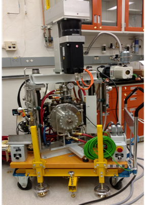
- Two (2) 5-ton systems capable of producing specimens of up to 1 inch (2.54 cm) in diameter. One of them is custom built for use in an x-ray radiography cave at INL, and in-situ analyses of microstructural evolution during material processing is possible. This an important tool for process development for new and current materials formulations.
- A 25-ton system capable of generating parts/samples with a 3-inch (7.62 cm) maximum diameter.
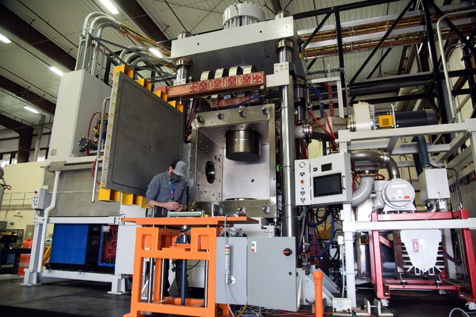
- The world’s largest EFAS (SPS) system, purposefully designed for industrial scale-up activities, capable of generating parts/specimens of up to 24-inch (60.96cm) diameter.
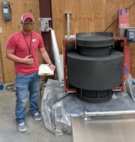
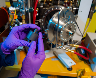
These machines and capability can be used to produce specimens as well as net-shape and near-net-shape parts for automotive applications. The capability is versatile enough to manufacture pure metal, metal alloy, metal matrix composite, ceramic matrix composite and carbon-carbon composite specimens and parts (net-shape and near-net-shape). EFAS/SPS affords small grain-sized materials owing to the speed at which sintering takes place. Flawless diffusion bonding of materials is also possible with no visible seamlines. Heat affected, mixed, and unmixed zones are absent, with no formation of dendrites. EFAS/SPS specimens and parts are smooth and require minimal post-processing. Auto components like full-size, fully dense, silicon carbide brake discs for light trucks have been produced on the largest system.
When applied, processing times, energy costs and unit cost per part can be reduced by up to 90% compared with traditional methods owing to extremely fast processing speed and the use of direct, rather than radiant, heating of the specimen/part.
Capability Bounds
- Nano EFAS/SPS: Beamline capability with generation of 3D tomographs to elucidate chemical and structural evolutions.
- Dr. Fuji System: 5-Ton Force Max, 1,500 Amps Max, 6 Volts Max, 2500°C, Max Operating Temp, 1 inch (2.54 cm) Max Sample Size.
- DCS-5: 5-Ton Force Max, 2,000 Amps Max, 9 Volts Max, 2500°C Max Operating Temp, 0.8 inch (2.0 cm) Max Sample Size, X-ray radiography capable, In-situ analyses of microstructural evolution during material processing capable.
- DCS-25: 25-Ton Force Max, 10,000 Amps Max, 9 Volts Max, 2500°C Max Operating Temp; 0.8-3.0 inch (2.0-7.62 cm) Sample Size.
- DCS-800: 800-Ton Force Max, 150,000 Amps Max, 9 Volts Max, 2500°C Max Operating Temp, 8-24 inch (20-60.96 cm) Sample Size, 64 cubic ft (4' x 4' x 4') Chamber.
Machines are capable of processing materials with melting points much higher than 2500°C when needed (owing to pressure-assisted solid state process).
Unique Aspects
- Nano/Micro to industrial scale (full spectrum) capable.
- Largest EFAS/SPS system in the world, with 24-inch diameter specimens/parts capable.
- Lightweight and extremely high temperature materials processing capable including pure metals, alloys, MMC, CMCs and C-C composites.
Availability
Available for collaborative or subcontracted efforts with INL researchers.